The 555 timer is an incredibly versatile integrated circuit that finds application in a myriad of electronic circuits. It can be used as three distinct types of oscillators because it has the flexibility to generate a repetitive waveform for different purposes.
But before we continue, what really is an oscillator?
At its core, an oscillator is a circuit that generates a repetitive, periodic waveform – an electronic heartbeat, if you will.
But why is this heartbeat essential? Oscillators serve a pivotal purpose in electronic circuits by providing the rhythmic pulses necessary for signal generation, timing, and synchronization.
Types of 555 Oscillator
In its Monostable mode, 555 functions as a precise timer with a predetermined time duration. Monostable oscillators are often used in applications requiring precise timing, such as in delay circuits or pulse generators.
Alternatively, when connected in Bistable mode, it exhibits a flip-flop switching behavior. This configuration is useful for applications where a stable on/off condition is required, such as toggling an output or memory storage.
To create a very stable oscillator circuit, the 555 timer IC should be configured in Astable mode. This configuration generates a highly accurate, free-running waveform. It’s also commonly used in applications such as clock generation, pulse-width modulation, and tone generation.
How Does the Astable 555 Oscillator Work?
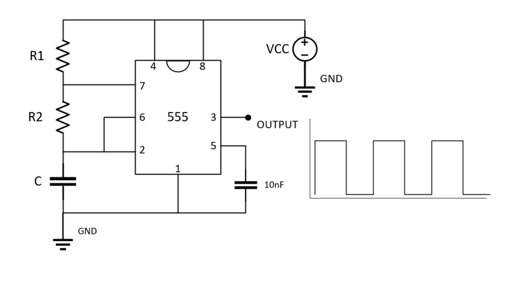
Let’s take a look at the circuit above. The capacitor C undergoes charging through the resistors R1 and R2.
And when the voltage across the capacitor reaches \(2/3\) of the supply voltage Vcc, pin 6 detects this condition and turns the output off. When the output goes off, pin 7 switches on and the capacitor discharges through R2.
Now, as the voltage across the capacitor drops to \(1/3\) of Vcc, pin 2 detects it and turns off pin 7, allowing the capacitor to start charging again. This completes the on/off cycle.
Also, note that a resistor is incorporated to protect pin 7 from potential damage when it turns off.
Oscillation Period
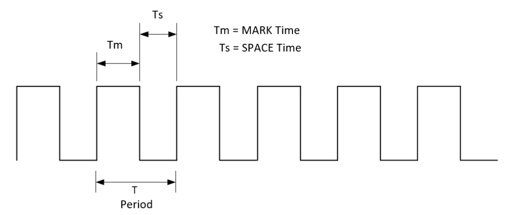
The period is the total time it takes to complete one cycle, as shown in the figure above. We can split the period into two parts.
MARK time (Tm) as the duration during which the output is HIGH and SPACE time (Ts) as the time when the output is LOW.
The formula for the period (T) can be expressed as:
\[ \large \text{T} = \text{T}_m+\text{T}_s \]
Where:
Tm = 0.693 x (R1+R2) x CTs = 0.693 x R2 x C
The formula can then be simplified as:
\[ \large \text{T} = 0.693 \cdot (R_1+2R_2)\cdot C\]
Frequency
As for the frequency, it refers to the number of cycles occurring within one second. In a flashing LED circuit, this controls how fast the LED blinks.
We can just take the reciprocal of the period (T) to determine it. But by rearranging the equation above, we can express the output frequency as:
\[ \large f \approx \frac{1.44}{(R_1+2R_2)\cdot C} \]
Duty Cycle
The duty cycle, on the other hand, refers to the ratio of the time the output is high (Tm) to the total time of a one complete cycle (T). It has no unit and is often expressed as a percentage.
\[ \text{DC} = \large\frac{T_m}{T} = \frac{R_1+R_2}{R_1+2R_2}\normalsize\cdot \text{100%} \]
Note that this formula generally assumes the space time (Ts) is much smaller than the mark time (Tm), providing a duty cycle of at least 50% or more. Also, in this configuration, it’s impossible to obtain a duty cycle of exactly 50%.
The oscillation frequency and the duty cycle can be adjusted by selecting appropriate values for R1, R2, and C.
- By decreasing R2, you’re increasing the mark time (Tm) which makes the duty cycle increase towards 100%.
- By increasing R2, you’re increasing space time which makes the duty cycle decrease towards 50%.
However, from this concept, please note that the duty cycle can only vary between 50% to 100%. That is because the timing capacitor charges through R1 and R2 but only discharges through R2.
How to Obtain a Duty Cycle of Less than 50%.
In a typical astable 555 oscillator circuit, we can’t get a duty cycle of less than 50% with the presence of R2. So, to obtain it, we can connect a signal bypass diode in parallel with resistor R2 as shown in the figure below.
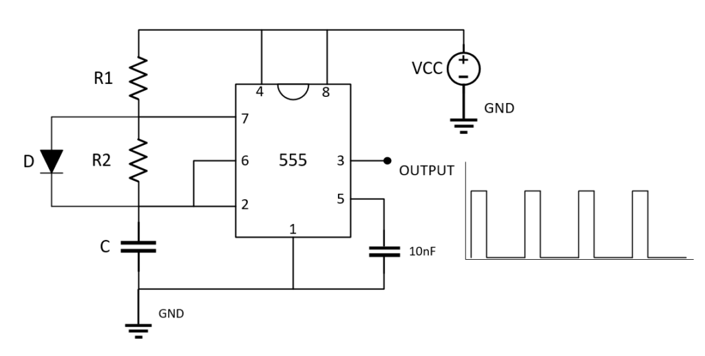
After connecting a diode (D) parallel to R2, the capacitor will now only charge through R1 because the diode effectively bypasses resistor R2 during the charging process. The capacitor still discharges through R2 as usual.
So, the new charging time (Tm) is now modified to \(0.693(R_1 \times C)\) due to this altered charging circuit. The duty cycle then becomes \( \large\frac{R_1}{(R_1 + R_2)} \).
In addition, to achieve a duty cycle of less than 50%, the value of R1 should be smaller than R2.
Astable 555 Oscillator Application: Flashing LED
To observe a 555 oscillator in astable mode, let’s put in it a real time application.
A basic 555 astable oscillator involves connecting a few components to the 555 timer IC. You only need timing resistors (R1 and R2) and a timing capacitor (C).
Choosing RC components for astable configuration:
1. Select a common capacitor value based on the desired frequency. Common values include 1μF, 10μF, or other values depending on the application. I’m going to chose 1μF as my capacitor value.
2. Calculate the combined resistance, \( Rt = (R_1 + 2 \cdot R_2)\), that will produce the desired frequency. In this case, I want my circuit to produce a frequency of around 3Hz.
\[ R_t = \frac{1.44}{f\times C} = \frac{1.44}{3 \times 1\,\mu\text{F}} = 480\,\text{k}\Omega \]
3. Next is I’m going to select the value for R1 first. I’m going to go with 1K for R1. Then this leads R2 to be either 240k ohms or 220k ohms. I’m going to select 220k ohms for R2.
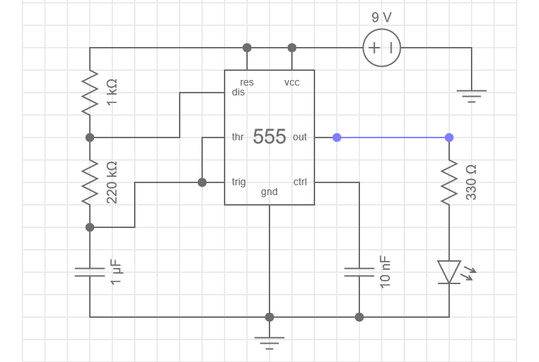
ⓘ Tip
You need to choose a significantly higher value for R2 than R1 to obtain a duty cycle as close to 50%.
Suppose R1 = 1k, R2 = 220k and C = 1μ, by calculation, the frequency is 3.2Hz. As for the Duty cycle, the calculated value is 50.11%. This is very close to my desired output so I’m not going to change anything.
Now, to complete the circuit, I’m going to include an LED with a current limiting resistor (R3) of 330 ohms for visual output. I’m also connecting a 10nF capacitor to pin 5. Finally, I’m going to set the Vcc to 9 Volts as shown in the figure above.
The video below shows a simulation I made in everycircuit.com to observe the real time waveform output of the circuit. Here, we can see that the waveform cycles 3 times per second. This means that the output goes on and off three times in a second.
Creator and Editor at AnitoCircuits.com based in Toronto